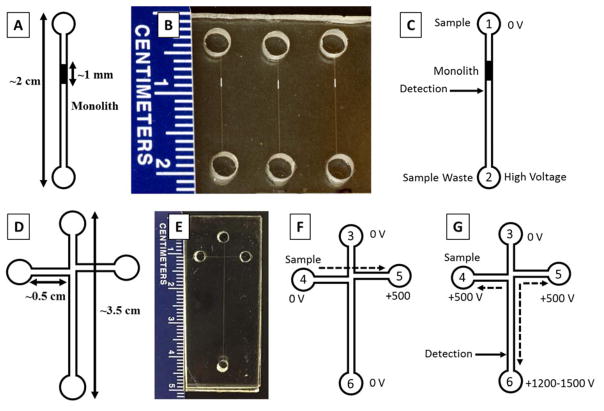
Figure 1.
Device layouts, photographs, and operation. (A) Device layout, (B) photograph and (C) operation of straight channel design showing sample reservoir (1), sample waste reservoir (2), voltage configuration and detection point used for on-chip labeling/SPE of PTB biomarkers. (D) Device layout, (E) photograph, and operation of “T” shaped device for μCE of PTB biomarkers showing (3) buffer, (4) sample, (5) sample waste, and (6) separation waste reservoirs along with voltage configuration and detection point for (F) injection and (G) separation in μCE.

