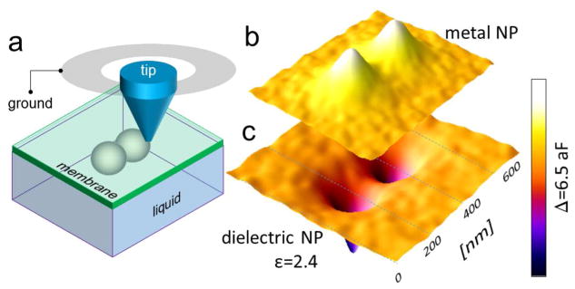
Figure 4.
(a) Schematic layout of the 3D model used to calculate capacitance maps shown in (b) and (c). Diameter of the spherical particles is 300 nm, membrane thickness is 8 nm, and permittivity is 9. The particles are immersed in water and are in contact with the membrane. Simulated probe-sample capacitance maps over pairs of (b) dielectric and (c) metallic particles. Permittivity of the dielectric particle material is 2.4. The full range of the color scale for capacitance is 6.5 aF. Probe-membrane contact radius was 20 nm in the models.

