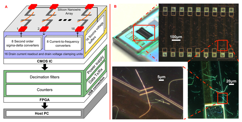
Figure 1.
(A) Building blocks of the overall sensing system and circuitry units of the CMOS readout chip. The nanowire sensor array is monolithically integrated directly on the CMOS chip, which has been mounted on a printed circuit board (PCB). The CMOS chip outputs are processed and then transmitted to a host PC by a FPGA. The acquired data are visualized and stored on the host PC with the help of a C# software interface. (B) Photograph of the CMOS chip highlighting the area where the SiNWs have been transferred to. SEM images at different magnifications of the SiNWs and of the electron-beam patterned Ti/Pd/Ti leads are shown. The diameters of the SiNWs amount to 20 nm.

