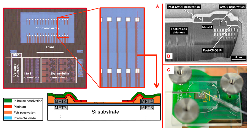
Figure 2.
(A) Micrograph of the fabricated CMOS chip with zoom-in on the integrated contacts (before the Pt deposition) used to connect the SiNWs to the circuitry. A sketch of the cross-section between a contact pair is also shown. (B) Focused-ion beam (FIB) cut through the CMOS chip in vicinity to the nanowire contacts: (left) featureless area between the contacts for deposition of nanostructures; (right) the 4 aluminum metal layers including vias of the CMOS chip and the post-CMOS Pt layer, which then serves as an inert electrical contact to the nanostructures in the featureless area. The bright top Pt layer has only been deposited for the FIB cutting. (C) Photograph of a complete and packaged system for experiments with liquid solutions. A PMMA cover clamps the PDMS block onto the chip/PCB surface; the inlet and outlet liquid ports are also visible.

