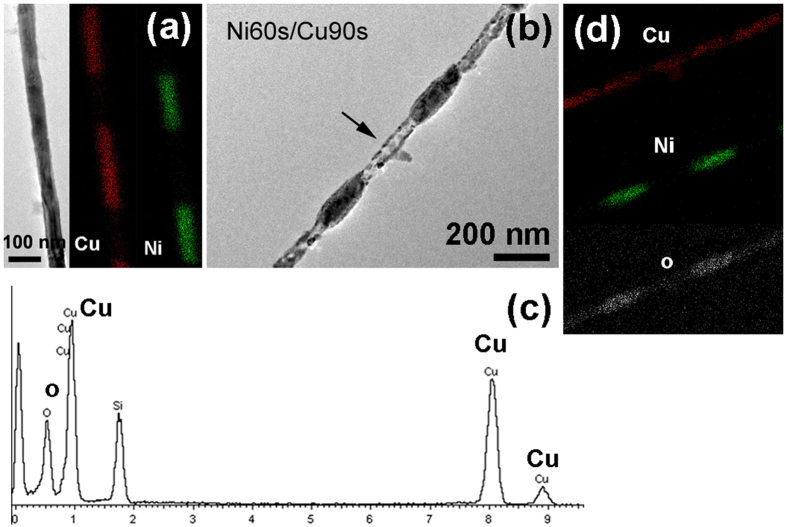
Figure 3.
Characterization results of Ni60s/Cu90s sample. (a) The TEM and element EDS mapping image of the single nanowire; (b) the same nanowire after annealing at 700 °C for 2 h in air. (c) EDS result of the tubular structure that has been labelled by arrow in (b); (d) EDS mapping image of the nanostructure in (b).

