
Figure 5.
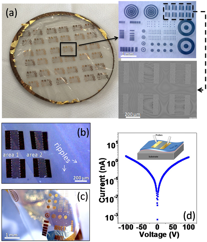
(a) BN wafer after device fabrication. Insets are microscope image of the metal contact patterns and scanning electron microscopy image of interdigitated electrodes. (b) Microscope image showing the local part where the film was separated from the substrate (area 2). (c) A small piece of freestanding BN prototype membrane lifted by tweezers which folded presenting the flexibility of the film. (d) Typical dark current-voltage (I-V) characteristics of the fabricated device prototypes and inset is the schematic of the measurements.