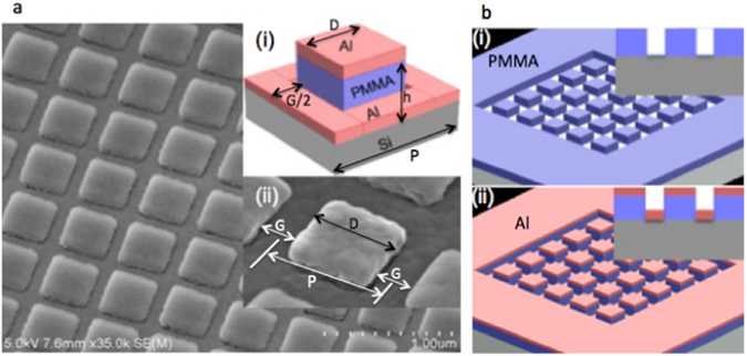
Figure 1.

SEM image of the plasmonic pixels in the 2D array structure and its simple fabrication process steps. (a) SEM image of the Al square patches hovering on PMMA nano pillars periodically arranged in a square lattice in the background of a fishnet like Al back reflector, insets (i) shows the schematic rendering of a single plasmonic color element and (ii) the slightly tilted (tilt angle of 20°) close-up SEM image of the single colour element. (b) Simple fabrication process involving (i) the patterning of 150 nm thick PMMA resist spin coated onto a piece of (100) silicon wafer using EBL. The exposed area of the resist is removed in a developer solution leaving PMMA nano pillars (inset shows the cross-sectional view). (ii) A 45 nm thick aluminum thin film is thermally evaporated onto the nano pillars for realizing vivid full colour pallets.
