
Figure 1.
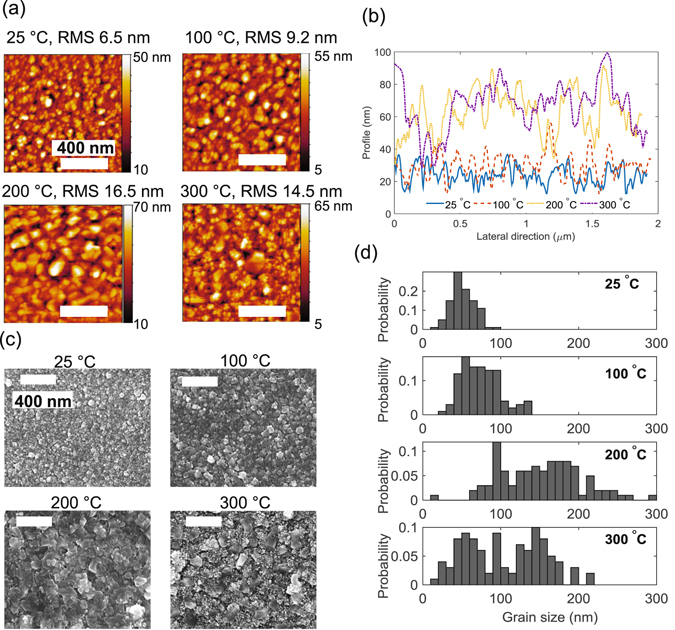
(a) Topography of the Al electrodes observed with AFM showing the effect of temperature on roughness, (b) Lateral cut profile across the AFM images showing increased roughness and grain sizes with T S < 300 °C, (c) SEM images of the Al displaying the increased grain sizes as temperature increases and a mixture of large and small grains at 300 °C and (d) Histogram of the grain size distribution of the Al electrode at different sputtering temperatures. All scale bars in (a,c) represent 400 nm.