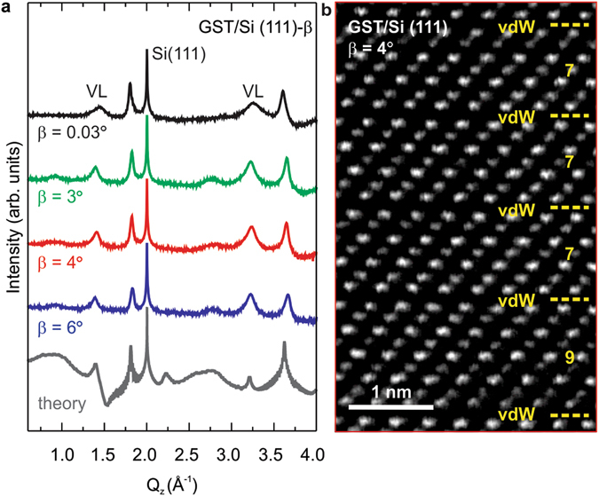
Figure 1.

The vicinal surfaces allows for high crystalline quality chalcogenides with reduced structural disorder. (a) X-ray diffraction (XRD) ω-2ϑ scans for crystalline GeSbTe (GST) grown on Si (111) with a miscut orientation (β) of 0.03° (black), 3° (green), 4° (red), 6° (blue). The substrate miscut improves the FWHM of the vacancy layer (VL) peaks. The gray curve is the simulation of GST grown on miscut. (b) Cross-view [11–20] high resolution HAADF-STEM micrograph of epitaxial GST (00.1) on Si (111) with β = 4°. Van der Waals (vdW) gaps (dashed yellow lines) occur every 7–9 atomic layers.
