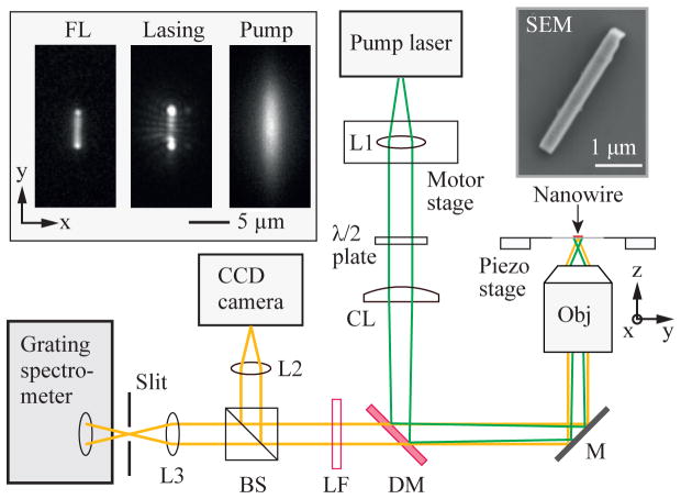
FIG. 3.
Schematic of the experimental setup. L1, L2, L3: spherical lenses, λ/2: half-wave plate, CL: cylindrical lens, DM: dichroic mirror, M: mirror, Obj: objective lens (NA=0.8, water immersion), LF: long pass filter, and BS: Beam splitter. SEM: a scanning-electron-microscope image of a typical lead iodide perovskite nanowire. Insets (from left to right): a typical fluorescence image of a perovskite nanowire below threshold, a stimulated emission image above threshold of the nanowire, and a pump beam profile recorded in the CCD camera.

