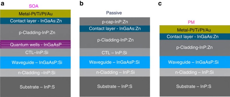
Figure 2. The epitaxial structures of the components in the proposed microring laser.
(a) The epitaxial structure of the SOA region, which has five QWs above the CTL. (b) The epitaxial structure of the passive waveguides without metal contacts, which are used for low-loss passive waveguide propagation sections. (c) The epitaxial structure of the phase modulator (PM) region, in which the CTL is removed to provide efficient current injection into the waveguide for high efficient phase tuning. Layer thickness: 150 nm contact layer, 1.7 μm p-cladding, 0–250 nm CTL, 300 nm waveguide and the QW layer contains 65 Å QWs and 80 Å barriers.

