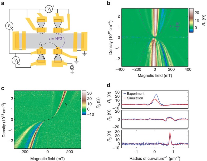
Figure 3. Probing edge scattering.
(a) Non-local resistance measurement schematic. (b) Resistance map characterizing angular profile of injected trajectories. A central peak near B=0 corresponds to the beam passing straight across the width of the device (a small angular offset is due to fabrication imperfections). The remainder of the electron-doped regime (n>0) is nearly featureless, whereas the hole-doped regime (n<0) has several auxiliary peaks. Dotted lines correspond to cyclotron orbits with radius equal to the half of device width (r=Wdev/2); features outside the two parabolas cannot correspond to direct ballistic trajectories between injector and collector. (c) Collimated transverse electron focusing. A sharp feature at r1=1.25 μm corresponds to trajectories that pass through four pinholes. Features at higher magnetic field must involve specular reflections off of the device edge. There is no such feature on the electron side, whereas there is a noticeable band on the hole side. (d) Comparison of experimental data with classical ballistic simulation. Experimental data (blue) are taken at n=2.7 × 1012 cm−2 and simulation (red) assumes fully diffuse edge scattering and 67% ohmic transmission.

