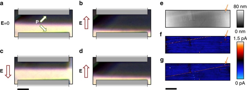
Figure 4. Electric field control of conducting domain walls near the Curie temperature.
(a) Polarized light microscopy of a conducting domain wall under zero applied field (E). (b) E-field applied between surface planar electrodes (schematized in grey) in positive sense causes wall to move towards bottom electrode. Arrows labelled P denote domain polarization direction. (c) Reversing applied field direction causes the wall to move towards the top electrode. (d) Field applied again in positive direction causes wall to move back towards the bottom electrode. The scale bar for a–d measures 25 μm. Topography, (e) and spatially resolved current map (f) of the conducting wall shown in a before switching fields are applied. (g) Spatially resolved current map of the conducting wall after switching shows that its transport properties are not changed by wall movement. The orange arrow points to a topographical marker which serves as a reference for relative wall position. The apparent ‘beaded' profile of the conducting wall is an imaging artefact due to the cantilever scan axis being at an oblique angle to the wall. For nanoscale current imaging, a bias of −10 Vdc is applied to the bottom electrode. The scale bar for e–g measures 10 μm.

