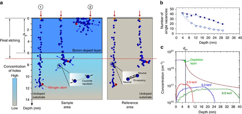
Figure 1. Simulated implantation defects in diamond and the proposed p+–i structure.
(a) Individual implantation sites (indicated by red arrows) simulated by MD with 4.0 keV nitrogen kinetic energy are shown representing different contributions of ion channelling. Blue dots represent implantation-induced vacancies, whereas red dots represent the rest position of implanted nitrogen atoms. A schematic representation of the novel method of nitrogen implantation across a planar p+–i junction is shown with the corresponding experimental steps (see left): boron-doped surface layer (6 nm) produced by CVD overgrowth, nitrogen implantation followed by thermal annealing and the final plasma etching step to remove the sacrificial boron-doped layer (7 nm)—the final fabricated region is named as ‘Sample area' in the main text. The concentration of free charge carriers (holes) in the substrate is represented by the blue–grey colour scale. The reference area is also shown, where vacancies are found mainly in the neutral charge state. (b) Depth dependency of single vacancies counted at each implantation site (squares) or confined in defect clusters of nanometre radius (see Supplementary Note 1) around nitrogen atoms at rest (circles) extracted from the MD simulations. (c) 1D depth profile of boron acceptors (blue-solid line) and free holes (dark red-solid line) across the p+–i junction structure at 950 °C by numerical simulation. Profiles of implanted nitrogen atoms for three different energies (2.5, 5.0 and 9.8 keV) simulated by CTRIM are shown for 3°-off implantation angle in a [100]-oriented diamond lattice (ion fluences of 1011 cm−2).

