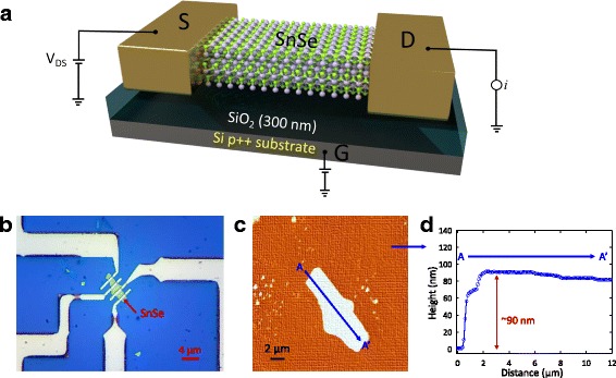
Fig. 3.

a Schematic of a mechanically exfoliated SnSe nanoflake FET on a SiO2/p++ Si substrate. b Optical image of a fabricated SnSe nanoflake FET that was used for electrical transport measurements. c AFM image of a SnSe nanoflake on a SiO2/Si substrate. d AFM height profile of a SnSe nanoflake, for estimating the thickness of, and fabricating FET devices
