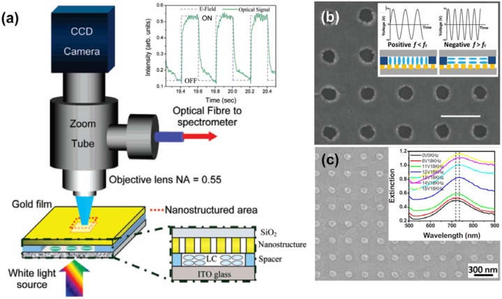
Figure 5.
(a) Schematic and experimental setup of a plasmonic switch consisting of nanostructures and liquid crystals. Electric field is generated by applying voltages across the gold film and bottom ITO glass, switching effect at the wavelength of 670 nm is shown in the inset; (b) SEM image of nanohole array and the working mechanism of DFLC. The scale bar indicates one period length of 300 nm; (c) SEM image of gold nanorods of another design of plasmonic switch using DFLC. The inset extinction spectrum shows the plasmonic resonance change under different voltage and frequency combinations. Figure 5a–c is adapted from reference [55], reference [47] and reference [50], respectively.

