Figure 2.

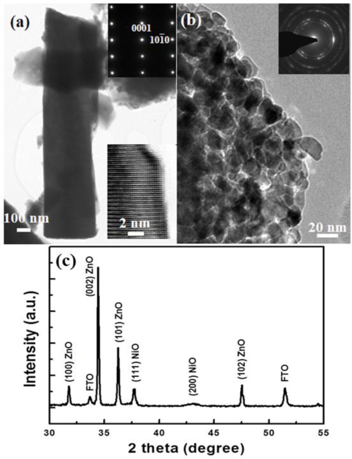
(a,b) TEM images with corresponding selected area electron diffraction (SAED) patterns of ZnO NR and NiO, respectively; (c) X-ray diffraction pattern for composite nanostructures of NiO/ZnO.

(a,b) TEM images with corresponding selected area electron diffraction (SAED) patterns of ZnO NR and NiO, respectively; (c) X-ray diffraction pattern for composite nanostructures of NiO/ZnO.