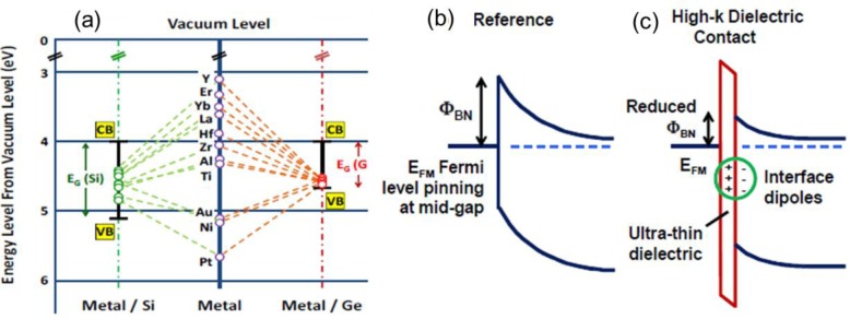
Figure 9.
(a) Most metal-semiconductor contacts result in Fermi level pinning to mid-gap on Si and the valence band edge on Ge; (b) fermi level pinning at mid-gap results in a large Schottky Barrier Height (SBH) adding resistance; (c) inserting a dielectric layer at the interface reduces MIGS penetration resulting in less Fermi level pinning and SBH can be further tuned by interface dipoles. Reprinted with permission from [132]. Copyright 2012 IEEE.

