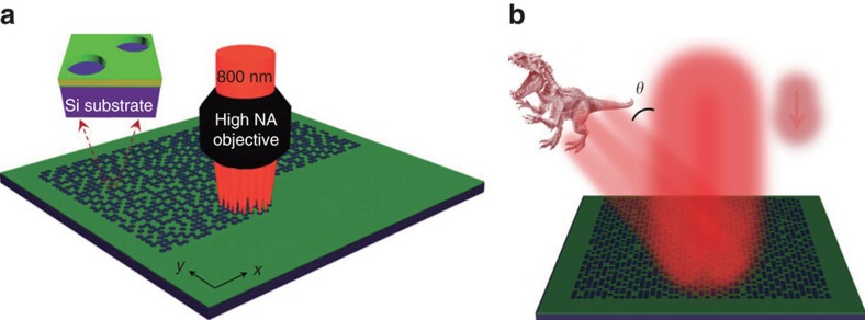
Figure 1. Nanofabrication of the binary hologram and holographic imaging procedures.
(a) Nanofabrication process of a nanometric Sb2Te3 hologram using the direct laser write system. The upper inset displays the ablated pixels in the topological insulator thin film. (b) Holographic imaging procedure of a nanometric Sb2Te3 hologram using a continuous wavelaser beam. θ is the projection angle of the holographic image. Note: this figure is not included under the article CC BY licence; Indominus Rex image is reproduced with permission from the publisher Comingsoon.net and copyright owner Universal Studios.

