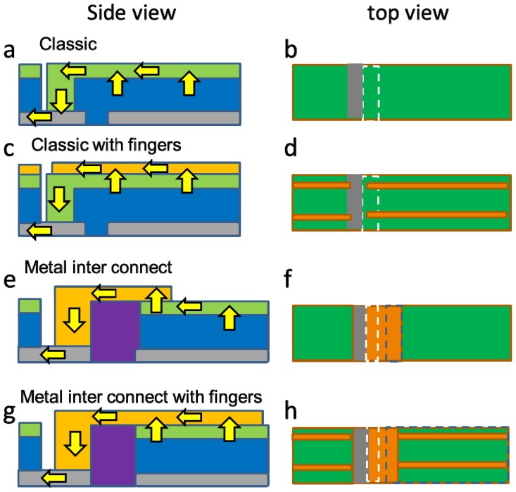
Figure 1.
Schematic representations (not to scale) of different interconnection and cell layouts with a side view (a,c,e,g) and a top view (b,d,f,h). The top image shows the front contact (in green), the absorber material (in blue) and the back contact (in grey). In addition, the separation and interconnection layout between two adjacent cells is shown. The surface area of the TCO/back contact material interface is indicated by the white dashed box. The flow of current is depicted by the arrows. The second highest image shows the case where the front contact is supplemented by a metal grid (in orange), whereas the right image displays the area covered by the metal (not to scale). The third image shows the case of the metal interconnect, for which two material interfaces are important: the metal back contact area represented by the white dashed box and the metal/TCO contact areas represented by the blue dashed box.

