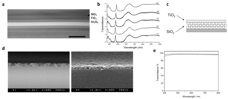
Figure 2.
(a) TEM micrograph of a TiO2 = Al2O3 bilayer on the Si wafer. The native SiO2 layer of ∼1:5 nm can be observed. The scale bar is 200 nm; (b) Transmittance spectra of the multilayer coatings for narrow-bandpass filters of the five dichroic filters. The spectra are offset by one for clarity. The dotted curves correspond to the experimental data, and the plain curves correspond to the calculated spectrum. The bandpass wavelength is shifted from 469 to 485 nm (Adapted with permission from [35]. Copyright 2009, The Optical Society); (c) Schematic view of double-layered TiO2–SiO2 with antireflective properties; (d) Cross-sectional electron micrographs of (PDDA/SiO2)6 and (PDDA/SiO2)6/(PDDA/nanosheet)6 multilayer films after calcination at 500 °C, respectively; (e) Calculated (triangles) and measured (dotted line) normal incidence transmission spectra of a TiO2–SiO2 double-layered film prepared from a (PDDA/SiO2)6(PDDA/nanosheet)9 multilayer assembly. The calculation was based on a 6.5 nm thick TiO2/55 nm thick SiO2 double-layered structure. (Adapted with permission from [36], Copyright 2006, American Chemical Society).

