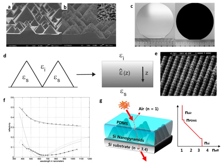
Figure 4.
Cross-sectional SEM photographs of (a) silicon pyramids created with KOH etching and (b) hierarchical structures generated with Ag-assisted etching. Inset: magnified SEM image; (c) Photographs of the polished silicon wafer (left) and the hierarchically structured silicon wafer (right) [91]. (Adapted with permission from [91]. Copyright 2009, American Chemical Society); (d) In a long wavelength limit, textured surface can be treated as a layer with gradually changing dielectric permittivity tensor [89]. (Adapted with permission from [89]. Copyright 2013, The Optical Society); (e) Scanning electron micrograph (SEM) photograph of a 260 nm-period 2D grating etched into silicon; (f) The upper solid curve and the dashed curve correspond to the reflectivity of a silicon substrate, without coating and with an antireflection quarter-wave, thin-film coating, respectively. The dashed-dot curve corresponds to the reflectivity of a silicon substrate corrugated by an ideal binary 2D SWS surface with a 100 nm thickness and a 0.5 fill factor. These three curves are obtained for normal incidence. The reflectivity measurements include light scattered into a 20° revolution cone around the specular reflection direction. These results are for an angle of incidence of 8° (Copyright IOP Publishing. Reproduced with permission from [92]. All rights reserved); (g) Structure and effective refractive index profiles of Si nanostructure deposited via PDMS [93]. (Adapted with permission from [93]. Copyright 2014, Springer).

