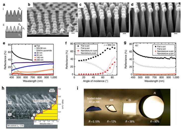
Figure 5.
(a) Schematic (i) tapered antireflection nanotexture and (ii) tapered nanotexture with graded refractive index; (b) 70° Angle cross-sectional scanning electron microscope (SEM) image of close-packed alumina nanostructures formed by infiltrating a 99 kg-mol−1 cylindrical phase polystyrene-b-poly(methyl methacrylate) block copolymer. Scale bar, 20 nm; (c,d) 70° cross-sectional SEM images of nanotextures fabricated by (c) 60 s and (d) 100 s of plasma etch. Scale bar, 20 nm; (e) Measured reflectance versus λ for a flat Si film, an 80 nm thick silicon nitride film and nanotextures with ℓ = 52 nm and t ranging from 32 to 230 nm. Also shown is the simulated reflectance of an 80 nm thick silicon nitride film on chemically etched inverted pyramids; (f) Measured reflectance (at 650 nm) for s- and p-polarization versus incidence angle for flat silicon (black circles) and nanotextures with ℓ = 52 nm and t = 230 nm (red triangles); (g) Measured reflectance of s- and p-polarization versus λ (45° incidence angle) for nanotextures with ℓ = 52 nm and t = 230 nm height (Adapted with permission from [108]; Copyright 2015, Nature Publishing Group); (h) Cross-sectional SEM image of graded-index coating with a modified-quintic-index profile. The graded-index coating consists of three TiO2 nanorod layers and two SiO2 nanorod layers; (i) Photograph of a graded-index antireflection coating on AlN and the specular surfaces of AlN, Si and Al (Adapted with permission from [109]. Copyright 2007, Nature Publishing Group).

