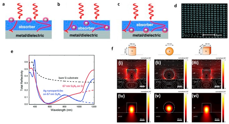
Figure 7.
Generalized scatterers for coupling into waveguide modes in a solar cell. Scatterers can consist of particles on the top (a); middle (b); or back (c) of the solar cell and could contain layers of metal, dielectrics, transparent conducting oxides, or air on the back surface. Incident sunlight is then scattered into photonic or SPP modes depending on the scattering object and incident wavelength of light (Adapted with permission from [134] Copyright 2010, John Wiley and Sons); (d) The SEM image of a silver nanoparticle array, fabricated by EBL; (e) Measured total reflection spectrum from a 300 μm crystalline Si cell coated with 67 nm Si3N4 (red) and the same sample with an optimized Ag particle array on top (blue). The particles reduce the reflection for wavelengths above 800 nm, improving the incoupling of light into the Si substrate. The dashed lines are extrapolated data representing the reflection from a semi-infinite substrate. The calculated reflectance of a semi-infinite Si substrate is shown for reference (dashed black line) (adapted with permission from [129]; Copyright 2011, American Chemical Society); (f) (i–iii) Vertical crosscuts through the center of all three particles in the plane parallel to the E-field of the source, showing the normalized |E|2 (color) and electric field lines (gray). The particle surroundings and air-substrate interface are indicated with white dashed lines. The respective geometries are shown above the figures. The displacement current loops are clearly visible (iv–vi). The same crosscuts as in (i–iii), now showing the normalized |H|2 (color) of the MD modes. The magnetic field lines are not plotted since H∼0 in this plane (perpendicular to source H⃗) (adapted with permission from [135]; Copyright 2013, The Optical Society).

