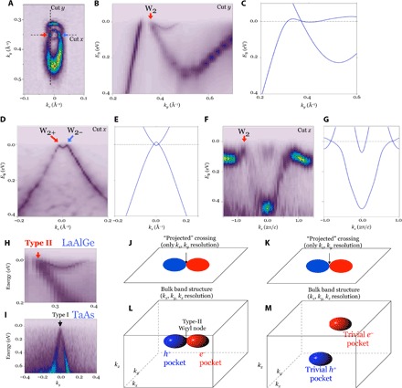
Fig. 3. Type II Weyl fermions in LaAlGe.

(A) The kx − ky Fermi surface map revealing a pair of type II W2 Weyl nodes in the form of touching points between electron and hole pockets. (B) Measured and (C) calculated E − ky dispersion maps along the cut y direction denoted in (A), which clearly resolve the W2 type II Weyl node at the crossing of two bands with the same sign of Fermi velocity. (D) Measured and (E) calculated E − kx dispersion maps for the direction along the cut x in (A). Here, the two type II W2 Weyl cones with opposite chirality nodes are resolved simultaneously. The photon energy used in the measurements presented in (A), (B), and (D) is 542 eV. (F) Measured and (G) calculated E − kz dispersion maps along cut z, showing that the W2 Weyl cone also disperses linearly along the out-of-plane kz direction. (H and I) ARPES dispersion maps showing the difference between the type II Weyl fermions of LaAlGe and type I Weyl fermions of TaAs, respectively. (L) The Fermi surface of a type II Weyl semimetal where electron and hole pockets touch to form the type II Weyl node. (J) The projected Fermi surface shows a crossing between the projected electron and hole pockets. (M) We have a completely different scenario in the bulk. The electron and hole pockets are separated at different kz values. (K) However, on the surface, their projections can still touch. This example clearly shows that the observation of a crossing in the projected band structure on surface does not mean a crossing in the bulk. The red and blue ellipsoids represent the electron and hole Fermi surfaces in the bulk BZ, respectively. The red and blue ellipses are the surface projection of the bulk Fermi surfaces.
