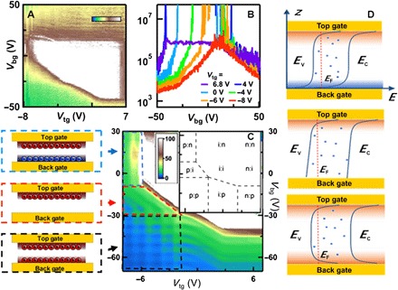
Fig. 2. Transport data.

(A and B) R(Vbg, Vtg) and line traces R(Vbg) at different Vtg at T = 1.7 K and B = 0. Note the logarithmic color scale (in Ω). (C) Right: R(Vbg, Vtg) at T = 0.5 K and B = 18 T, featuring a complicated quantum oscillations pattern. The color scale is in kΩ. Left: Schematics of the charge distributions that correspond to bipolar double-layer, single-layer, and unipolar double-layer regimes, respectively. Inset: Charge types for top and bottom surfaces at different combinations of gate voltages. p, hole-doped; n, electron-doped; i, intrinsic insulating state. (D) Band diagrams that correspond to the three regimes in (C), with dots illustrating mid-gap impurity states.
