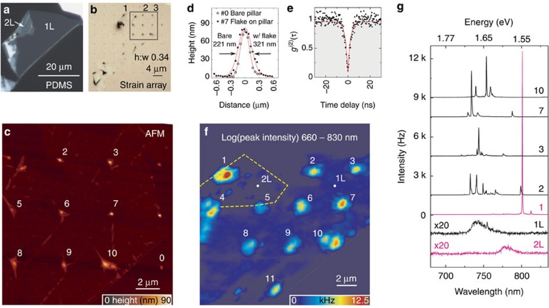
Figure 2. A monolayer WSe2 quantum emitter array.
Optical micrographs of an exfoliated 1L WSe2 flake (a) before and (b) after transfer onto an Si substrate with an array of dielectric nanopillars. The black box in b identifies the region shown in c and f. (c) AFM image of the topography of the flake on top of the nanopillars, revealing a lattice of locally strained points. (d) Cross-section AFM profile of a bare nanopillar #0 and nanopillar #7 that is covered by the monolayer. (e) Second-order photon correlation statistics from a typical 1L quantum emitter revealing clear antibunching [g(2)(0)=0.07±0.04 and τ=2.8±0.2 ns]. (f) Colour-coded spatial map of the peak PL signal in the spectral range of 660–830 nm. (g) Example PL spectra of isolated quantum emitters at the pillar locations as labelled. Also shown is the weak signal from the unstrained 1L and 2L WSe2.

