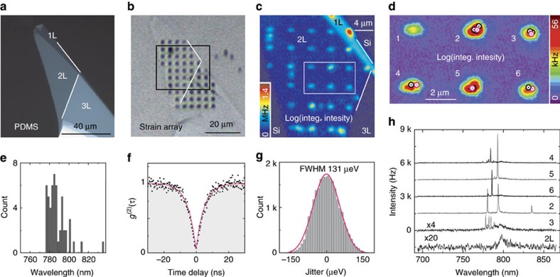
Figure 3. A bilayer WSe2 quantum emitter array.
Optical micrograph of 2L WSe2 (a) before and (b) after the transfer onto the nanopillars. (c) A 2D spatial map of the PL integrated intensity within 700–860 nm. (d) A high resolution spatial map of integrated intensity of the six nanopillars indicated in c. The red circles mark the positions of emitters in h. (e) A histogram of the wavelengths of the 2L WSe2 emitters. (f) Photon auto-correlation histogram from the bi-layer emitter at nanopillar #1 of Fig. 1. A fit using g(2)(0)=0.03±0.02 and τ=4.8±0.1 ns is shown. (g) A histogram of the spectral jitter over 20 h (3 s time-bin) of the emitter at nanopillar #1 of Fig. 1. (h) PL spectra from the emitter positions identified in d with red circles.

