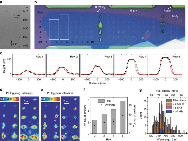
Figure 4. Optimization of strain-induced arrays of quantum emitters.
(a) A 45° SEM image of an SiO2 substrate with an array of nanopillars of varying aspect ratios, as labelled. (b) Optical micrograph of a large (100 × 25 mm) 1L WSe2 flake covering 101 nanopillars. Some high aspect ratio nanopillars exhibit a dark centre with a bright ring, which suggests the pillar punctured the flake during the transfer process. (c) Cross-section AFM profiles of bare nanopillars from different rows with varying aspect ratio. (d) High-resolution colour-coded spatial map of integrated PL signal in the spectral range of 690–850 nm for columns 2–5 from the region outlined in b. For the flake at nanopillars with higher aspect ratios there is a clear ring in the PL intensity. (e) Same maps as d showing the peak intensity where the individual emitters are resolved. (f) Statistics on the emitters per pillar for each row where each error bar represents a single standard deviation from the mean. (g) Histogram of the emitter wavelengths with post-selection on the emitter brightness (peak intensity at 0.8 saturation level).

