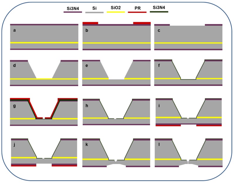
Figure 1.
Cross-sectional schematic flow for the production of a single solid-state nanopore. (a) Deposition of 2 µm Si3N4 on both side of SOI wafer using PECVD; (b) patterning photoresist on backside of SOI wafer; (c) removal of exposed Si3N4 using RIE; (d) anisotropically etched Si using 30% KOH; (e) removal of SiO2 using 5 wt % HF; (f) sputtered 200 nm Si3N4 on Si (n-type); (g) patterning photoresist on n-type; (h) removal of exposed Si3N4 using RIE; (i) patterning photoresist on front side of the SOI wafer; (j) removal of exposed Si3N4 using RIE; (k) formation of v-shaped groove cavity on front side and square cavity on rear side of Si (n-type) using a low concentration of KOH; and (l) formation of a nanopore in thin silicon membrane using an electrochemical setup.

