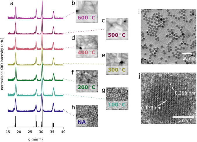
Figure 1.

Nanocrystal structural characterization. (a) XRD spectra for drop-cast and annealed films of Cu2Se. In this plot, q is in units of 2π/d. The reference peaks are calculated from the room temperature structure determined by Gulay et al.37. (b–h) Top-view SEM images of thin films that were annealed at the same temperature as the drop-cast samples used for XRD spectra in (a). In panel (h), “NA” stands for “not annealed”. Each image is 170 nm across. (i) Low resolution TEM image of Cu2Se nanocrystals. (j) High resolution TEM image of a Cu2Se nanocrystal.
