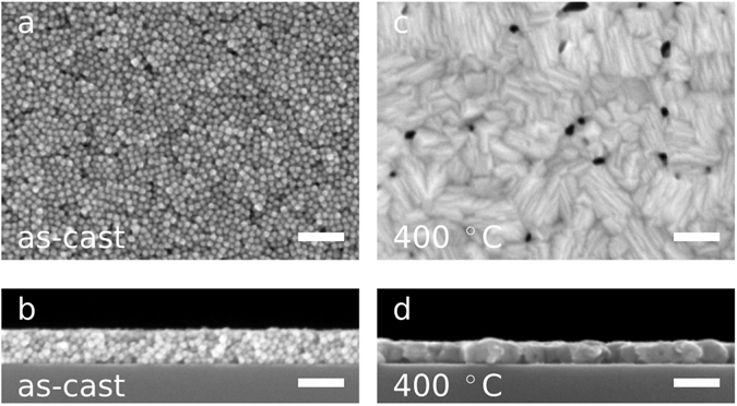
Figure 2.

Thin Film Morphology. (a) Top-view SEM image of an as-cast thin film of Cu2Se nanoparticles. (b) Cross-section SEM image of the film shown in (a). The film is 75 nm thick. (c) Top-view SEM image of a Cu2Se thin film after annealing at 400 °C for 45 minutes in an N2 atmosphere. Prior to annealing, this film was prepared the same way as the film in (a). (d) Cross-section SEM image of the film shown in (c). The film is 54 nm thick. The scale bars in all images are 100 nm wide. The full sets of top-view and cross-section SEM images are shown in Supplementary Figures 2 and 3.
