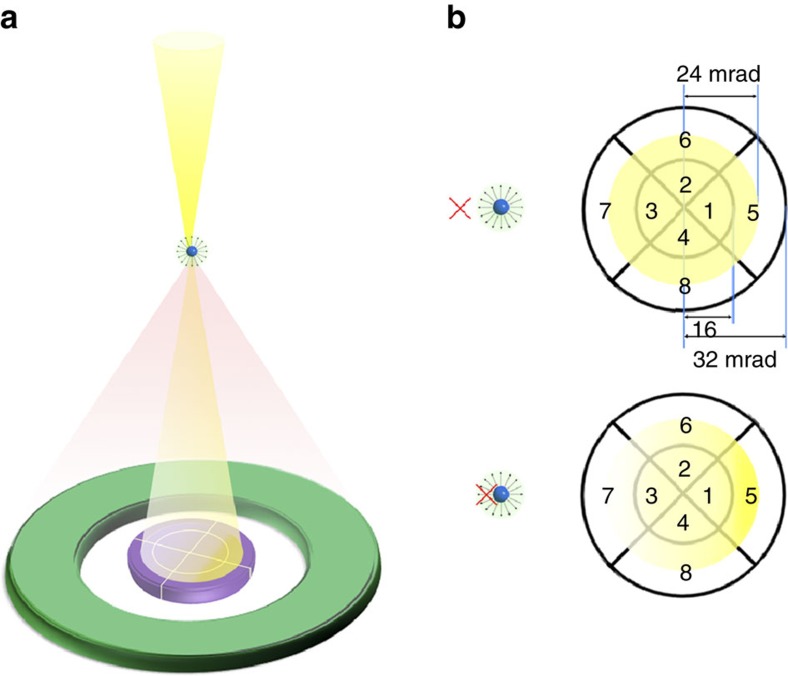
Figure 1. Schematic illustration of detector geometries in atomic-resolution STEM.
(a) The large-angle doughnut-shaped detector (green) selectively collects electrons scattered to high angles by atoms to form atomic-resolution ADF STEM images. The segmented detector (purple), inserted in the bright-field region of the illuminating cone, sensitively detects atomic electric fields. (b) Schematic illustration of the bright-field disk intensity distribution on the segmented detector for two different electron probe positions, as indicated by red crosses, near an atom. When the probe position is away from the atom (upper figure), the bright-field disk intensity is uniform. When the probe position is in the vicinity of the atomic centre (lower figure), the intensity distribution changes because of the interaction of the electron probe with the perpendicular component of the atomic electric field (pointing radially from the atomic nucleus) as projected along the incident electron beam direction. The intensity change on the different detector segments can be used to determine the in-plane atomic electric field of an atom or atomic column.

