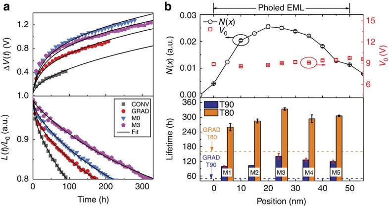
Figure 4. Lifetime and modelling of the PHOLEDs.
(a) Lifetime characteristics of CONV, GRAD, managed PHOLEDs M0 and M3. Top and bottom show the time evolution of the operating voltage change, ΔV(t)=V(t)–V0, and the normalized luminance degradation, L(t)/L0, respectively. Solid lines are fits based on the model in Methods (see fitting parameters in Table 2). (b) (Top) Exciton density profile, N(x), of the PHOLED emission layer (EML) as a function of position, x, and operating voltages of the devices using delta-doped sensing layer at J=5 mA cm−2 (Supplementary Note 3). The origin of the x-axis is at the HTL/EML interface. The operating current density results in a luminance of L0=1,000 cd m−2. (Bottom) Lifetimes (T90 and T80) of managed devices (M1–M5) as functions of the position of the managed EML zones. T90 and T80 of the managed devices are compared with those of the GRAD (dotted lines). Note that the variation in lifetime qualitatively follows the exciton density profile, suggesting that placing the manager at the point of highest exciton density results in the longest device lifetime. Error bars represent 1 s.d. for at least three devices.

