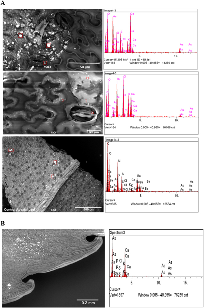
Figure 3.

(A) SEM-EDX mapping of the abaxial surface of As (V) treated leaflet treated with 13.3 mM AsV. SEM images of PV pinnae (left) showing crystalline deposits. Multiple spots on each sample (marked by red squares) were analyzed by EDX (right). Top Panel: Arsenic-treated pinna before extraction, Middle Panel: As-treated pinna after extraction, Lower Panel: Control pinna (untreated). (B) SEM-EDX mapping of the adaxial surface of As (V) treated leaflet treated with 13.3 mM AsV. Spots on were analyzed by EDX (right).
