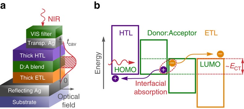
Figure 1. Working principle of the original cavity enhanced organic photodetector.
(a) Simplified scheme of the device architecture with a sketch of the optical field distribution for the resonance wavelength in the NIR. The thickness of both transport layers is chosen to achieve constructive interference in the CT absorption band and to situate the D:A blend layer in the maximum of the optical field. Layer thicknesses are not drawn to scale. (b) Simplified energy diagram at open circuit. A photon with less energy than the optical gaps and at least the CT state energy ECT is absorbed at the interface between an electron donating semiconductor and C60 as acceptor. Thereby, an electron in an occupied state on the donor is promoted into an unoccupied state on the acceptor. The resulting intermolecular CT state dissociates into a free electron and hole which are extracted via the electron (ETL) or hole transport layer (HTL) at the respective Ag electrode.

