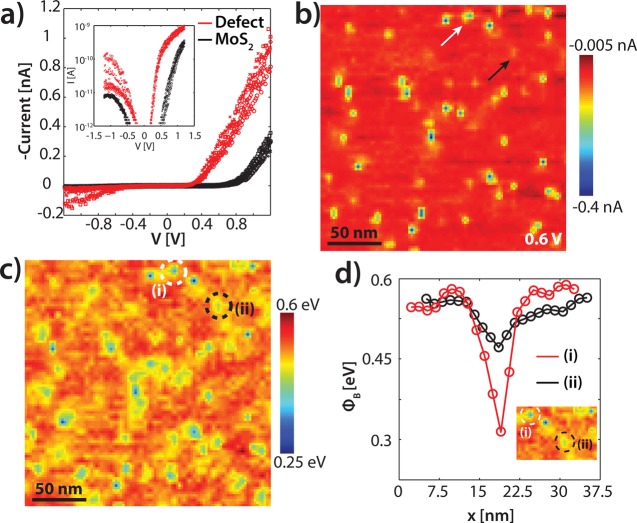
Figure 3.
(a) I(V) curves recorded with a doped diamond tip on the pristine MoS2 surface (red) and on a defect (black). The different symbols represent different measurements. Inset: The corresponding semi logarithmic I(V) curves. (b) A spatially resolved current map (200 × 200 nm2) obtained via 128 × 128 grid I(V) curves, recorded from −1.2 to 1.2 V. The map corresponds to a voltage of 0.6 V. The white arrow indicates a metal-like defect located at the first trilayer, whereas the black arrow a metal-like defect located at the second trilayer. (c) The extracted Schottky barrier height (ϕB) map of the surface obtained by the I(V) curves in (a). Significant variations are observed that are induced by subsurface defects. (d) Cross sections of the ϕB taken above subsurface defects of the first (red) and second (black) MoS2 trilayers indicated with dashed white and black circles in the inset. Inset: the corresponding ϕB map.

