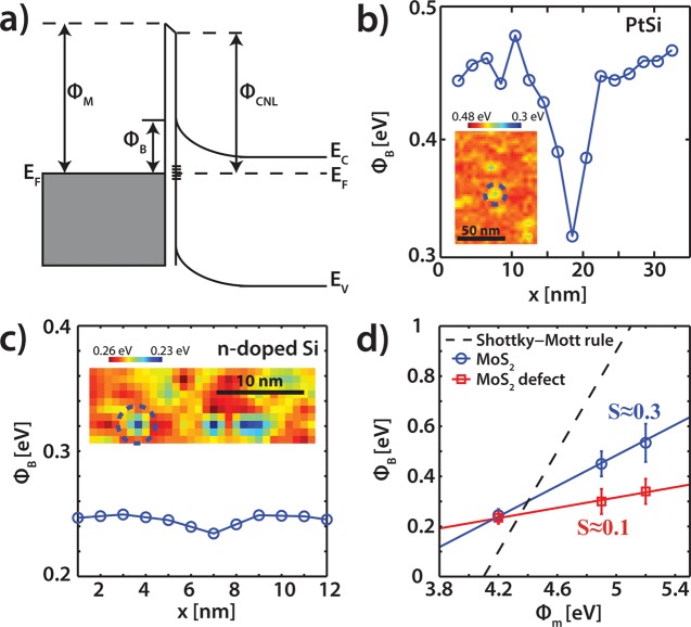
Figure 4.
(a) Schematic of a metal–semiconductor junction with a Schottky barrier including Fermi level pinning. (b) Cross section of the spatially resolved ϕB map above a first trilayer subsurface defect, recorded with a PtSi tip. Inset: the corresponding ϕB map. (c) Cross section of the ϕB map for a subsurface defect recorded with a n-doped Si tip. Inset: the corresponding ϕB map. (d) Schottky barrier height for the pristine MoS2 (blue) and the defects (red) for various work functions of the tip (ϕM). The pinning factor S and the charge neutrality level (ϕCNL) are extracted using eq 6. The dotted line is the standard Schottky–Mott rule (see eq 1).

