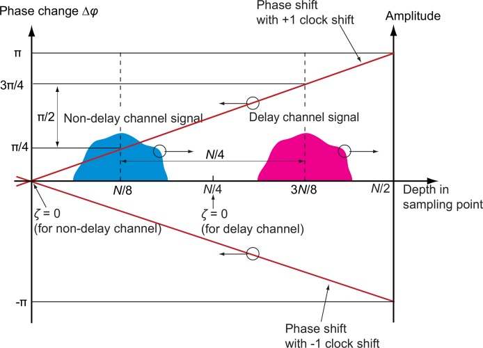
Fig. 2.
Schematic diagram of the phase shift caused by the random shift of the spectral sampling signal. N is sampling number and ζ is indexed depth position. The 0-th sampling point corresponds to the zero depth of the non-delayed polarization channel, while N/4-th sampling point corresponds to that of delayed polarization channel. The upper and lower red lines indicate a phase error caused by jitter of +1 and −1 clock shifts, respectively. For the +1 clock shift, the delayed signal is phase shifted by +π/2 in respect to the non-delayed channel. For the −1 clock shift, the corresponding phase shift is −π/2.

