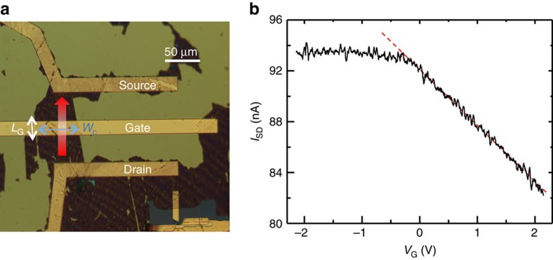
Figure 7. Field effect transistor and transport data.
(a) Optical microscope image of a top gate FET with a channel made by printing the water-based ink (W-GSA sample). (b) Dependence of the source-drain FET current (IDS) from the gate bias VG in the range from −2.2 V to +2.2 V, measured while a source-drain voltage VSD=1 mV is applied. The dashed line represents the fit to the data in the linear region and gives a transconductance∼4.4 nA V−1.

