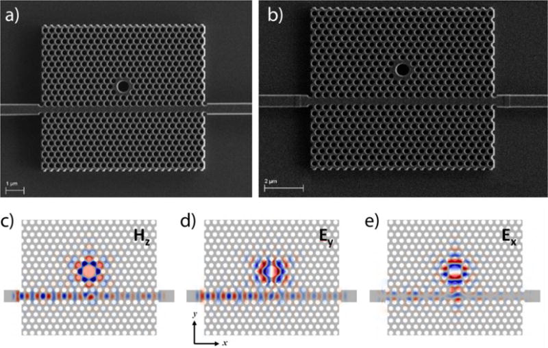
Fig. 1. PhC sensor geometry.

(a,b) Electron micrograph images of the two PhC sensor geometries used for these studies. The PhC geometries consist of a triangular lattice of low-RI holes, a W1 PhC waveguide traversing the lattice, and a large-hole, point-like lattice defect centered either 4 (a) or 5 (b) rows from away from the W1 waveguide. (c–e) Simulated electromagnetic field profiles of the photonic device shown in (a) at the resonant frequency of the optical mode used for sensing. Calculated using 3D FDTD methods, cross sections are taken at the center plane of the silicon device layer and demonstrate field localization around the large-hole defect of PhC.
