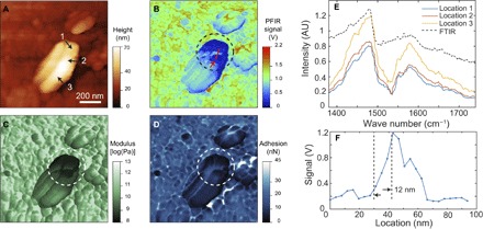
Fig. 4. PFIR imaging and spectroscopy on the perovskite crystal.

(A) The AFM topography of the surface of the CH3NH3PbBr3 perovskite crystal. A 500-nm × 300-nm nanocrystal is observed on the large perovskite crystal surface. (B) The PFIR image obtained of the region with the infrared frequency of 1585 cm−1. (C and D) The co-registered modulus and adhesion images of the region on the perovskite crystal. Clear inhomogeneity within the small nanocrystal can be identified from the infrared absorption map, modulus, and adhesion map. (E) PFIR spectra from three individual locations [marked as 1, 2, and 3 in (A) on the perovskite nanocrystal]. The FTIR spectrum of bulk perovskite crystals is shown as a reference (black dashed curve). (F) A section profile of the PFIR response from the perovskite crystal from the marked red line in (B). It demonstrates a spatial resolution of 12 nm, estimated from the width between 90 and 10% of the height of the signal.
