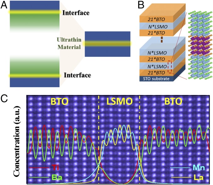
Fig. 1.
Designing ultrathin materials via interfaces. (A) When two interfaces are geometrically close enough, the confinement effect of two interfaces can lead to unexpected properties in the ultrathin films in between. (B) Stacking order of BTO/LSMO SLs. (C) HADDF STEM image and EELS elemental profiles extracted from La M (yellow), Ba M (green), Mn L (blue), and Ti L (red) edges for BTO/4uc-LSMO/BTO (n = 4) SL taken along [110] zone axis direction, showing sharp interfaces with minor intermixing. The dashed yellow lines mark the interfaces. For all of the STEM images, the STO substrate is located at the right side.

