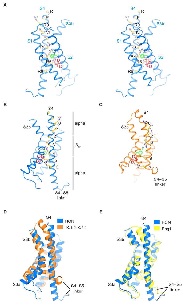
Figure 4. Voltage sensor of the HCN1 channel.
(A) Stereo view of the voltage sensor. Yellow spheres denote Cα positions of Arg252, Arg255, Arg258 (R0), Lys261 (K1), Ser264, Arg267 (R3), Arg270 (R4), Arg273 (R5) and Arg276 (R6). Resides that form the gating charge transfer center are labeled (Phe186, green; Asp189 and Asp225, red).
(B and C) Comparison of the HCN1 and Kv1.2–2.1 voltage sensors (PDB ID: 2R9R). The gray bars in (B) show the extents of α- versus 310-helical transitions in the S4 helix of the HCN1 channel.
(D) Superposition of the HCN1 and Kv1.2–2.1 voltage sensors using Cα atoms of S1 and S2 helices. The S1–S2 loop of Kv1.2-Kv2.1 is not shown for clarity.
(E) Superposition of the HCN1 and Eag1 voltage sensors (PDB ID: 5K7L), using Cα atoms of S1 to S3 helices.
See also Figure S6.

