
Fig. 1. Fabrication and characterization of ultrathin Ge nanomembranes on foreign substrates.
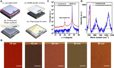
(A) Schematic of the fabrication process flow of the Ge nanomembranes on foreign substrates. The laboratory-made GeOI was used as the source wafer, and the membrane transfer–printing method (figs. S5 and S6) was then used to transfer the Ge membrane onto a foreign substrate. Subsequent thin-down process was adopted to obtain the desired Ge thickness (10 to 60 nm). (B) Optical microscopy image of ultrathin Ge (10 to 60 nm), which is transfer-printed on Al2O3/Ag/Si substrates. Scale bars, 75 μm for all five subfigures. (C) Triple-axis HR-XRD scans of our transferred crystalline ultrathin Ge (red) and evaporated amorphous Ge (blue) films. The thicknesses are both 20 nm. (D) Raman scattering results of the two samples in (C). The Raman signal of the transferred Ge membrane shows the typical single peak (300.9 cm−1) of single-crystalline Ge materials.