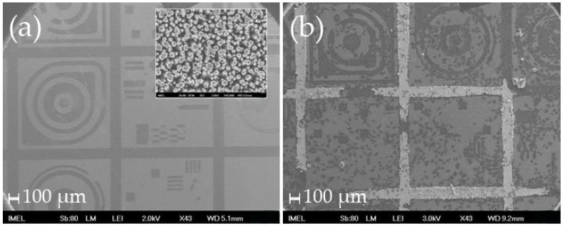
Figure 2.
SEM images of (a) of the patterned Si wafer with larger patterns and larger flat areas (the darker areas contain the ZnO nanorods shown in the zoom-in inset image; scale bar: 100 nm); (b) the same samples with HeLa cells after 4 days in culture, where one can see that the cells mostly adhere onto the flat areas (the white areas are the nanorods that have been covered by salts from the nutrient medium that was not fully removed after washing). Scale bar: 100 μm.

