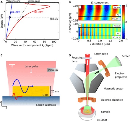
Fig. 1. Concept of SR-SPP imaging in 2PPE PEEM.

(A) Illustration of the SPP dispersion relations at gold-vacuum and gold-silicon interfaces. The dispersion relations are calculated from a 20-nm-thick gold film [with optical properties discussed by Johnson and Christy (38)] on a silicon substrate with a native SiO2 layer. λ0 = 800 nm (dashed black line) is the excitation wavelength for LR-SPPs (blue line) and SR-SPPs (red curve). Image (B) represents cross sections through the sample, together with the x component of the SPP electric field. In (i), LR-SPPs are illustrated, which are predominantly located at the gold-vacuum interface. In (ii), SR-SPPs are described, which mainly exist at the gold-silicon interface. They can extend to the gold-vacuum interface in the z direction if the gold thickness is small enough. (C) Illustration of the experimental concept: Single-crystalline gold platelets are deposited on silicon substrates. This allows SPP excitation at the material interfaces due to normal incident ultrashort laser pulses (<15 fs) of 800-nm wavelength with linear transversal magnetic (TM) polarization. LR-SPPs are indicated at the gold-vacuum interface (blue), and SR-SPPs are indicated at the gold-silicon interface (red). (D) SPP excitation and imaging are realized using two-photon photoemission microscopy at normal incidence. After SPP excitation, electrons are emitted from the sample and imaged with a nanometer resolution using electron optics. As recently demonstrated (41), the Ex component of the surface plasmon field along the incident polarization is responsible for the electron emission.
