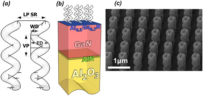
Figure 1.

(a) Schematic view of the single helix, with another neighbor element. The wire diameter (WD) is 110 nm, the external diameter (ED) is 300 nm, and the vertical pitch (VP) is 300 nm. The helix is supposed to have a perfectly round shaped cross section. The lattice period (LP) of the square array is 700 nm. (b) Schematic view of the substrate laying beneath the helices layer. It consists of a GaN/AlGaN heterostructure where a two dimensional electron gas allows for charge effect management during the helices growth by FIBID10, 24. All the heterostructure is epitaxially grown on a thick (380 micron) Al2O3 substrate. (c) scanning electron microscope (SEM) view of the sample.
