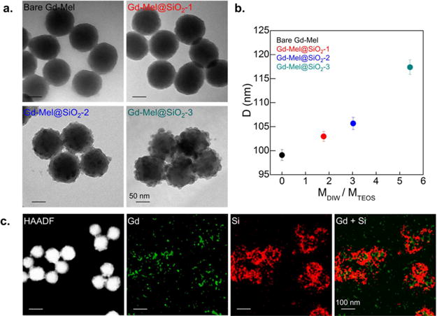
Figure 3.

(a) TEM images of as-synthesized Gd-Mel NP with controlled amount of silica nanocoating: the leftmost image shows bare Gd-Mel NP and rest three TEM images show controlled silica nanocoating on Gd-Mel NPs (Gd-Mel@SiO2 NPs), indicated as Gd-Mel@SiO2-1, Gd-Mel@SiO2-2, and Gd-Mel@SiO2-3 in each panel. (b) Diameter (D) of Gd-Mel@SiO2 NPs as a function of molar ratio of distilled water and tetraethyl orthosilicate (TEOS) (MDIW/MTEOS). (c) High-angle annular dark-field scanning transmission electron microscopy (HAADF-STEM) image of Gd-Mel@SiO2 NPs and elemental mapping images of gadolinium (Gd) and silicon (Si), respectively and their superposition of elemental maps of Gd and Si.
