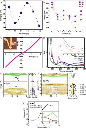
Fig. 2. Electronic properties and band structure of fluorinated boron nitride.

(A) Variation of bandgap calculated from the UV-vis absorption measurements with the percentage of fluorine doping. The bandgap was calculated from the absorbance measurements using Tauc plot. (B) Variation of deconvoluted PL spectra according to the percentage of fluorine doping. Each PL spectrum was deconvoluted into three peaks, namely, A, B, and C. (C) I-V curve obtained from two-probe measurements conducted on a device fabricated on fluorinated boron nitride (F-BN) on a silicon substrate with SiO2 coating. The inset shows an optical image of the device. (D) Magnetotransport measurements as a function of temperature at zero field, low field, and at high field. The inset shows the negative magnetoresistance at two different temperatures. (E and F) Band structures and density of states with atomic contribution obtained by spin-polarized calculations for F-BN sheets having (E) 6.25% and (F) 12.5% F concentrations. (G) Change in bandgap (Eg) as a function of F concentrations calculated from DFT calculations. Inset shows variation in defect level and valence band maximum (VBM) and conduction band minimum (CBM) from doping above 5%, where defect level is seen.
